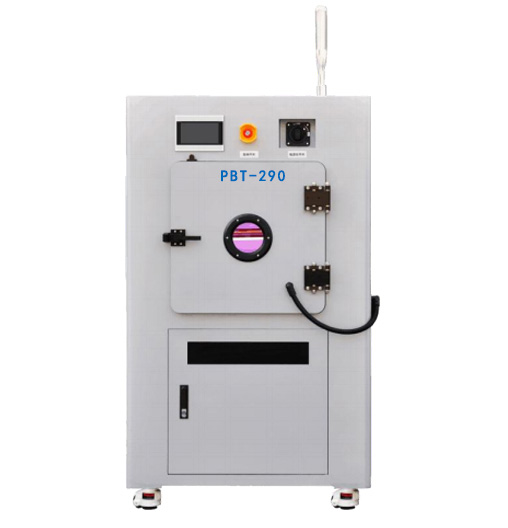
Process flow:
The gas is separated into plasma state by excitation power supply -- the plasma acts on the surface of the product -- cleaning the contaminants on the surface of the product -- improving the surface activity and enhancing the adhesion property.
Plasma cleaning is a new, environmentally friendly, efficient and stable surface treatment method.
Field of Application:
• Mobile phone industry: TP, middle frame, back cover surface cleaning activation;
•PCB/FPC industry: in-hole drilling and surface cleaning,Coverlay surface coarsening and cleaning;
• Semiconductor industry: Semiconductor packaging, camera module,LED packaging,BGA packaging,Wire Bond preprocessing;
• Ceramics: packaging, dispensing pre-treatment;
• Surface coarsing etching: PI surface coarsing,PPS etching, semiconductor silicon wafer PN junction removal,ITO film etching;
• Plastic materials :Teflon Teflon surface activation,ABS surface activation, and other plastic materials cleaning activation;
• Clean the surface before ITO coating.
Equipment features:
• Flexible product placement fixture, can adapt to irregular products;
• Horizontal electrode design to meet the needs of soft product handling;
• Low energy consumption gas products;
• Convenient way of retracting and releasing board;
• Integrated vacuum system, small footprint;
• Reasonable plasma reaction space, so that the treatment is more unifom;
• Integrated control system design to make operation more convenient.
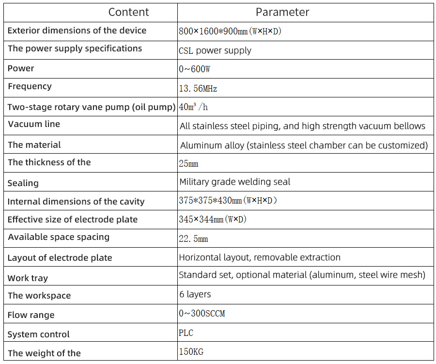
Technical parameters:
